Huawei Unveils Tau Scaling Law to Challenge Moore’s Law Amid Supply-Chain Curbs
At ISCAS 2026, semiconductor chief He Tingbo outlines an architecture-driven roadmap targeting 1.4nm-class effective density by 2031 through 'LogicFolding' and 'UnifiedBus.'
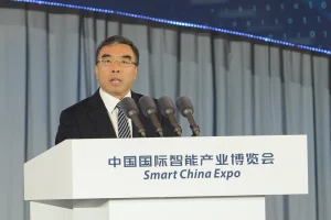
Shanghai — Huawei has introduced a semiconductor design framework aimed at improving system-level efficiency under constraints imposed by mature fabrication technologies and restricted access to leading-edge manufacturing equipment. The announcement was made at the IEEE International Symposium on Circuits and Systems (ISCAS), a major conference in circuit and systems engineering. The company outlined the “Tau (τ) Scaling framework”, alongside a circuit/layout methodology termed “LogicFolding” and a system interconnect architecture referred to as “UnifiedBus”.
Huawei claims this combined approach may, at a system level, achieve performance-density characteristics comparable to chips fabricated at more advanced future process nodes (such as a 1.4nm-class equivalent) by 2031. This should be interpreted strictly as a performance abstraction metric rather than a physical lithographic node, consistent with how modern semiconductor scaling discussions separate architecture from fabrication capability.
For more than five decades, semiconductor progress has been driven by geometric scaling under Moore’s Law and Dennard scaling, which rely on transistor miniaturization to increase density and performance. In contemporary semiconductor engineering, however, gains increasingly depend on system-level techniques including chiplet architectures, 3D integration, and EDA-driven physical design optimization.
These approaches reflect a structural shift where interconnect delay, power density, and packaging constraints have become dominant limiting factors in system scaling.
ALSO READ: Pope Leo XIV: Magnifica Humanitas & AI Disarmament
Within this context, Huawei’s Tau framework functions as a system-level abstraction model focused on reducing end-to-end signal latency (“temporal minimization”) across compute, memory, and interconnect layers. Rather than introducing changes at the fabrication level, it targets optimization across existing design hierarchies.
At the circuit level, LogicFolding is described as a layout optimization methodology intended to reduce critical-path wire length and associated resistive-capacitive (RC) delay. This aligns with conventional VLSI design objectives where interconnect minimization is a primary determinant of performance and energy efficiency.
The UnifiedBus component operates as a system interconnect architecture designed to reduce communication overhead across processing clusters. Functionally, this corresponds to established network-on-chip (NoC) and chiplet interconnect approaches used in modern heterogeneous computing systems.
Huawei reports approximately 381 chip implementations over the past six years using related methodologies. This figure has not been independently disaggregated into Tau-specific deployments and should be interpreted as an internal usage metric rather than externally validated performance evidence.
The company further projects that its architecture-centric approach could achieve “1.4nm-equivalent” transistor density by 2031. In semiconductor terminology, this does not correspond to a physical lithographic node defined by foundries such as TSMC, but instead represents a composite performance-density estimate combining architecture, interconnect efficiency, and packaging effects.
Leading semiconductor manufacturers such as TSMC continue to advance physical scaling through process technology development, while companies such as SMIC operate under more constrained access to advanced EUV lithography systems supplied by ASML. These constraints define the broader industrial context in which architecture-centric scaling strategies are emerging.
Initial deployment is expected in upcoming Kirin processor generations. Huawei reports internal improvements in density and efficiency metrics; however, these claims have not yet been independently validated through standardized third-party benchmarking or cross-fabrication comparison.
If externally verified, architecture-centric scaling approaches could demonstrate meaningful efficiency gains in constrained manufacturing environments. However, they remain bounded by fundamental semiconductor physics, interconnect scaling limits, and fabrication node constraints.